Photomask Market
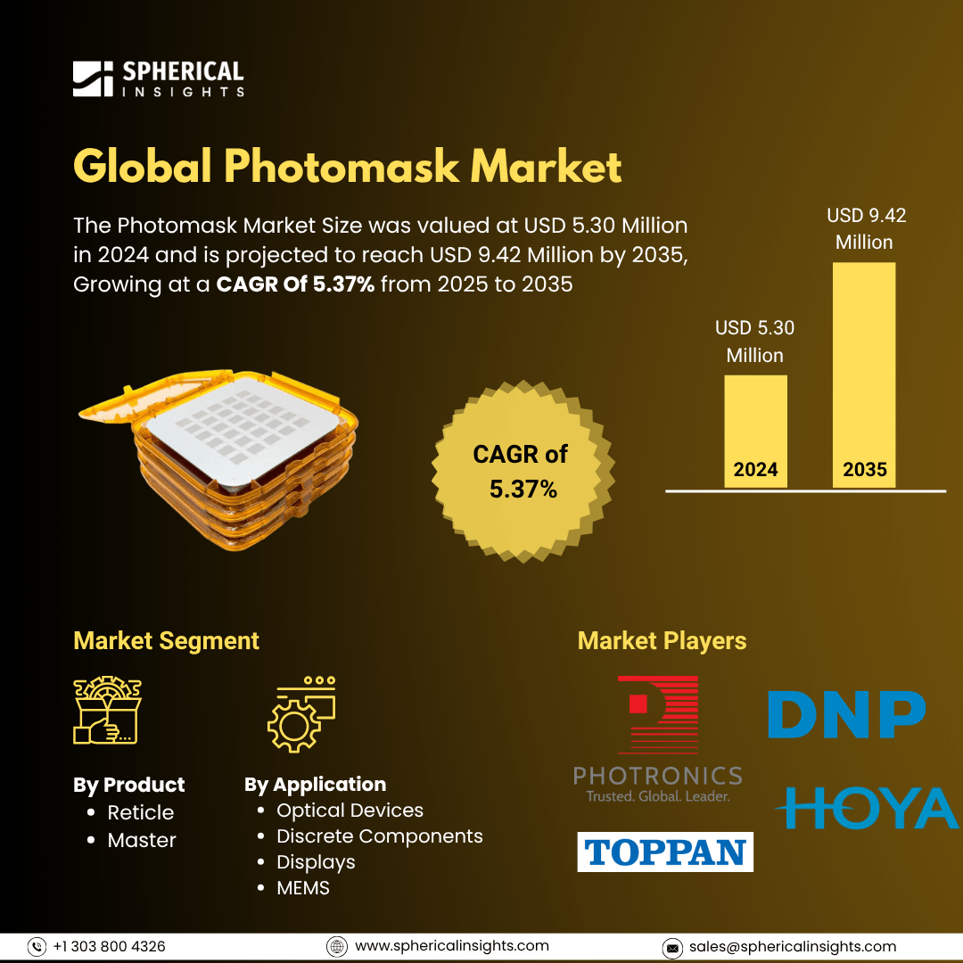
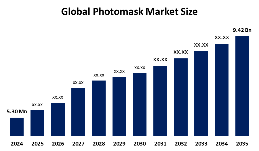
The Global Photomask Market Size was valued at USD 5.30 Million in 2024 and is projected to reach USD 9.42 Million by 2035, Growing at a 5.37% CAGR from 2025 to 2035. The global photomask market is a key segment of the semiconductor and electronics manufacturing industry, playing a crucial role in the photolithography process used to create intricate circuit patterns on semiconductor wafers. Photomasks are precision tools made from quartz or glass plates coated with patterned materials, essential in the production of integrated circuits, flat panel displays, and other microelectronic components. These masks are categorized into different types such as reticles, master masks, and working masks, each suited for specific applications. The market is segmented based on product type, technology, and end-use industries. Asia-Pacific leads the market due to its strong presence of semiconductor manufacturing hubs, followed by North America and Europe. The industry includes both merchant and captive mask suppliers, supporting a wide range of design and production needs.
Attractive Opportunities in the Photomask Market
- Increased collaboration among photomask manufacturers, semiconductor foundries, and equipment makers (e.g., IBM and Toppan's R&D partnership for EUV masks) enables faster innovation, cost-sharing, and customized solutions for next-gen semiconductor nodes (e.g., 2nm and beyond).
- Rapid semiconductor infrastructure development in emerging economies, particularly in Asia-Pacific, opens up opportunities for regional players to enter the market and participate in the global supply chain.
- The shift toward advanced chip packaging techniques, including 3D integration, creates a strong demand for high-precision photomasks. These technologies enable compact, high-performance chips essential for AI, high-performance computing, and mobile devices.
Global Photomask Market Dynamics
DRIVER: Increasing demand for more powerful and compact electronic devices
The global photomask market is growing steadily due to the increasing demand for more powerful and compact electronic devices. As technology advances, semiconductor chips need to be smaller and more complex, which requires highly detailed photomasks to create precise patterns on wafers. The rise of modern technologies like 5G, artificial intelligence (AI), and the Internet of Things (IoT) is pushing the need for better and faster chips, boosting the use of advanced photomasks. New methods such as Extreme Ultraviolet (EUV) lithography are also being adopted to keep up with these demands. Additionally, the expansion of semiconductor manufacturing facilities, especially in Asia, supports this growth. Companies are investing more in research and development to improve photomask technology, while partnerships among manufacturers and suppliers are helping the industry grow faster.
RESTRAINT: High cost of producing advanced photomasks, especially for technologies
One major issue is the high cost of producing advanced photomasks, especially for technologies like EUV lithography, which require expensive tools and strict cleanroom environments. As semiconductor designs become more complex, the risk of defects increases, leading to higher inspection and correction costs. Smaller companies may struggle to compete due to these financial and technical demands. Additionally, the market is sensitive to fluctuations in semiconductor demand and global supply chain disruptions, which can impact production timelines and material availability, further limiting consistent market expansion.
OPPORTUNITY: Growing demand for advanced packaging and 3D integration
One key area is the growing demand for advanced packaging and 3D integration, which requires highly precise photomasks to enable complex chip designs. Additionally, the rise of new applications such as flexible electronics and wearable devices opens new markets for photomask solutions. Innovations in materials and mask-making processes, including the development of reusable and defect-reducing photomasks, present chances to improve cost-efficiency and production yield. Expanding manufacturing capabilities in emerging regions offer opportunities for local players to enter the market and support global supply chains. Furthermore, increasing collaboration between photomask manufacturers, semiconductor foundries, and equipment makers can accelerate technological advancements and create customized solutions, driving long-term growth in this sector.
CHALLENGES: Photomasks for cutting-edge semiconductor nodes involves highly complex and precise processes
Producing photomasks for cutting-edge semiconductor nodes involves highly complex and precise processes, which increase production difficulty and costs. Maintaining defect-free masks is critical, as even minor imperfections can cause significant issues in chip fabrication, leading to higher rejection rates and increased waste. The market is also affected by the cyclical nature of the semiconductor industry, where fluctuations in demand can cause instability in production and investment. Furthermore, the long lead times required to design and manufacture photomasks can delay product launches for chipmakers. Supply chain disruptions, including shortages of raw materials and geopolitical tensions, add uncertainty and risk to the market. Additionally, the growing sophistication of lithography technologies demands continuous innovation, which requires substantial R&D investment.
Global Photomask Market Ecosystem Analysis
The global photomask market ecosystem involves several key players working together to support semiconductor manufacturing. Photomask manufacturers and sellers create and supply the masks used in chip production, collaborating closely with semiconductor foundries and integrated device manufacturers. Equipment and material suppliers provide the tools and raw materials needed for mask fabrication. Design houses prepare chip layouts for mask creation, while research institutions drive innovation. Logistics partners ensure timely delivery. This interconnected network enables the precise production and distribution of photomasks, essential for advancing semiconductor technology worldwide.
Based on the product, the reticle segment is expected to hold the highest revenue share during the forecast period
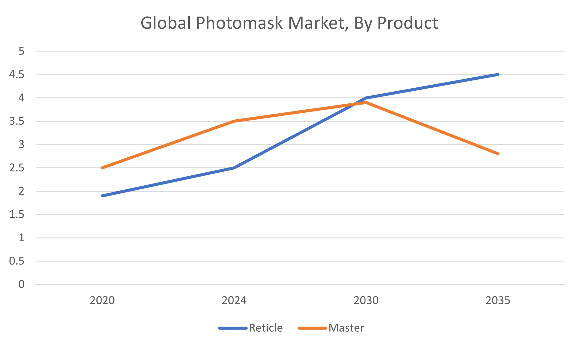
The reticle segment leads the global photomask market due to its vital role in advanced lithography processes like DUV and EUV. Reticles are large, detailed photomasks used repeatedly to transfer complex circuit patterns onto semiconductor wafers, essential for producing smaller, high-performance chips. As technology advances to smaller nodes like 7nm and 5nm, the precision required from reticles increases, making them indispensable in modern semiconductor manufacturing. The growing demand for powerful chips in technologies such as 5G, AI, and IoT further boosts the need for advanced reticles. This importance drives strong revenue growth and a significant CAGR for the reticle segment.
Based on the application, the displays segment accounted for the largest revenue share and is expected to grow at a substantial CAGR during the forecast period
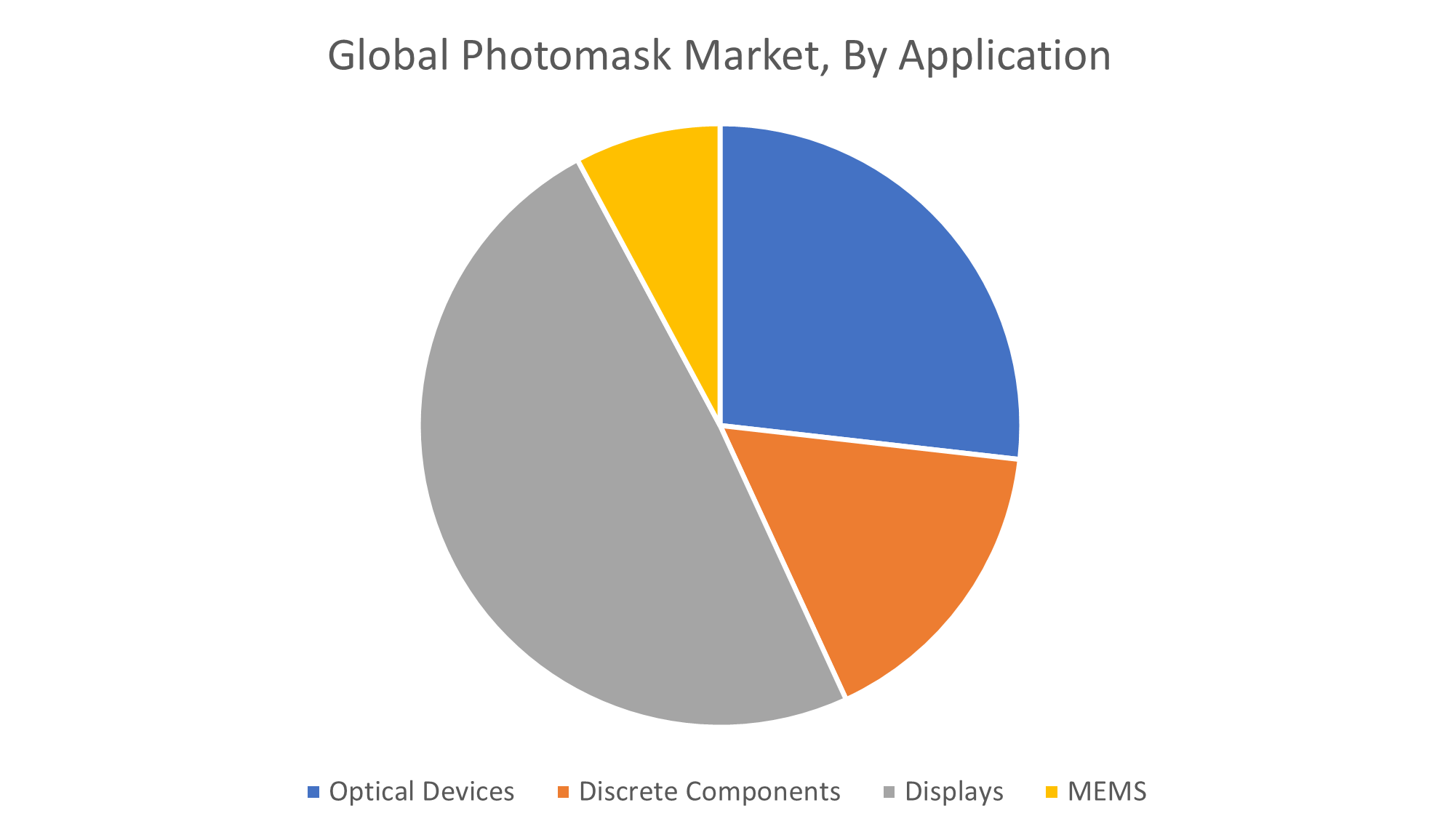
The displays segment has emerged as a leading force in the global photomask market due to its critical role in enabling cutting-edge screen technologies. Photomasks are essential for fabricating intricate circuit patterns in flat-panel displays like LCD, OLED, and AMOLED. As consumers increasingly seek larger, sharper, and more energy-efficient displays across smartphones, TVs, and wearables, the demand for high-precision photomasks in this sector grows rapidly. Moreover, expanding uses in automotive dashboards, digital signage, and healthcare devices create new opportunities. Innovations in flexible and foldable displays further boost this demand, driving strong revenue growth and a substantial CAGR for the displays segment over the forecast period.
Asia Pacific is anticipated to hold the largest share of the photomask market during the forecast period
Asia Pacific is expected to maintain the largest share of the global photomask market throughout the forecast period. This dominance is driven by the region’s strong semiconductor manufacturing base, with major players located in countries like Taiwan, South Korea, China, and Japan. These countries host some of the world’s largest semiconductor foundries and integrated device manufacturers, creating high demand for photomasks. Additionally, significant investments in advanced technology fabs and growing electronics industries further boost market growth. The presence of leading photomask manufacturers and suppliers in the region also supports its strong market position, making Asia Pacific a key hub for photomask production and innovation.
North America is expected to grow at a fastest CAGR in the photomask market during the forecast period
North America is set to register the fastest CAGR in the photomask market over the forecast period. This surge is largely fueled by the region’s strong emphasis on innovation and robust investments in semiconductor research and manufacturing. With major technology hubs and leading semiconductor companies headquartered in the U.S. and Canada, demand for advanced photomasks is rising to support emerging technologies like AI, autonomous vehicles, and 5G networks. Furthermore, government policies focused on boosting local semiconductor production and enhancing supply chain resilience are accelerating growth. Together, these elements position North America as a dynamic and rapidly expanding market for photomasks globally.
Recent Developments of the Photomask Market
- In February 2024, Toppan Photomasks, Inc. entered into an agreement of joint research and development with IBM. This agreement included research and development of EUV semiconductor photomasks. Furthermore, this agreement will help bring materials and process control skills of both the companies to provide commercial solutions for 2nm node and beyond printing.
Key Market Players
KEY PLAYERS IN THE PHOTOMASK MARKET INCLUDE
- Photronics, Inc.
- Dai Nippon Printing Co., Ltd. (DNP)
- Toppan Printing Co., Ltd.
- Hoya Corporation
- Taiwan Mask Corporation
- Compugraphics (a subsidiary of Photronics)
- SMEE (Shanghai Micro Electronics Equipment Co., Ltd.)
- NuFlare Technology, Inc.
- SUSS MicroTec SE
- LG Siltron
- Others
Market Segment
This study forecasts revenue at global, regional, and country levels from 2020 to 2035. Spherical Insights has segmented the photomask market based on the below-mentioned segments:
Global Photomask Market, By Product
Global Photomask Market, By Application
- Optical Devices
- Discrete Components
- Displays
- MEMS
Global Photomask Market, By Regional Analysis
- North America
- Europe
- Germany
- UK
- France
- Italy
- Spain
- Russia
- Rest of Europe
- Asia Pacific
- China
- Japan
- India
- South Korea
- Australia
- Rest of Asia Pacific
- South America
- Brazil
- Argentina
- Rest of South America
- Middle East & Africa
- UAE
- Saudi Arabia
- Qatar
- South Africa
- Rest of the Middle East & Africa