Global Atomic Layer Deposition Market Size, Share, and COVID-19 Impact Analysis, By Product Type (Metal ALD, Aluminium Oxide ALD, Catalytic ALD, Plasma Enhanced ALD, and Others), By Application (Electronics & Semiconductors, Medical Equipment, Research & Development Facilities, Fuel Cells, Solar Devices, Magnetic Heads, Sensors, Barrier Layers, Primer Layers, Optical Devices, Thermoelectric Materials, Non—IC Application, and Others), and By Region (North America, Europe, Asia-Pacific, Latin America, Middle East, and Africa), Analysis and Forecast 2021 - 2030.
Industry: Advanced MaterialsGlobal Atomic Layer Deposition Market Insights Forecasts to 2030
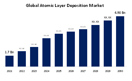
- The Global Atomic Layer Deposition Market Size was valued at USD 1.7 Billion in 2021.
- The Market is Growing at a CAGR of 12.5% from 2022 to 2030
- The Worldwide Atomic Layer Deposition Market Size is Expected to reach USD 4.90 Billion By 2030
- North America is Expected to Grow the fastest during the forecast period
Get more details on this report -
The Global Atomic Layer Deposition Market is expected to reach USD 4.90 billion by 2030, at a CAGR of 12.5% during the forecast period 2022 to 2030. The atomic layer deposition market has grown due to the growing utilization of novel materials and designs for improved chip production. In addition, the trend toward miniaturization is being embraced by industries all around the world. As a result, there is currently a higher need for tiny electronics and machinery.
Market Overview
The technique of depositing precursor materials on substrates to enhance or modify qualities, including chemical resistance, strength, and conductivity, is known as Atomic Layer Deposition (ALD). The procedure is regarded as a subset of chemical vapour deposition (CVD) in atomic layer deposition. Two chemicals—often precursors—are used in the reaction.
During the forecast period, increased demand for semiconductor chips, which are utilized in various electronic devices, is anticipated to boost industrial output. Materials are deposited using the atomic layer deposition (ALD) method when fabricating semiconductors. Governments worldwide are investing in and promoting the use of electric vehicles due to growing worries about global warming and environmental degradation. As a result, the market for lithium-ion batteries is expanding due to their potential as an energy source for automobiles.
The use of atomic layer deposition in lithium-ion battery manufacturing is having a favorable impact on the market's expansion. The increasing innovation and product development in solar cells, backed by increased investment in renewable energy technologies, is also anticipated to boost the expansion of the atomic layer deposition market. For instance, according to PV Magazine, Chinese producers use atomic layer deposition technology of solar cells.
The emergence of various novel and energy-efficient technologies has led to a rapid increase in the demand for small, portable gadgets. The creation of semiconductor chips frequently involves the use of atomic layer deposition techniques. Furthermore, the rising adoption of electronics and semiconductor technologies internationally boosts the market for atomic layer deposition. During the forecast period, the automotive industry will also influence the atomic layer deposition market.
Global Atomic Layer Deposition Market Report Coverage
| Report Coverage | Details |
|---|---|
| Base Year: | 2021 |
| Market Size in 2021: | USD 1.7 Billion |
| Forecast Period: | 2021-2030 |
| Forecast Period CAGR 2021-2030 : | 12.5% |
| 2030 Value Projection: | USD 4.90 Billion |
| Historical Data for: | 2019-2020 |
| No. of Pages: | 200 |
| Tables, Charts & Figures: | 120 |
| Segments covered: | By Product Type, By Application, By Region |
| Companies covered:: | Forge Nano Inc., Beneq Group, Oxford Instruments plc, The Kurt J. Lesker Company, Pico sun Oy, SENTECH Instruments GmbH, Arradiance, LLC, NCD Co. Ltd., Lam Research Corporation, ASM International, Applied Materials, Inc., Veeco Instruments Inc., and CVD Equipment Corporation |
| Growth Drivers: | The global atomic layer deposition market is expected to reach USD 4.90 billion by 2030, at a CAGR of 12.5% during the forecast period 2022 to 2030. |
| Pitfalls & Challenges: | The global repercussions of COVID-19 have demonstrated the significance of interconnection in international cooperation. As a result, many governments have been hurrying to find, assess, and buy trustworthy AI-powered solutions. |
Get more details on this report -
Report Coverage
This research report categorizes the market for global atomic layer deposition based on various segments and regions, forecasts revenue growth, and analyzes trends in each submarket. The report analyses the key growth drivers, opportunities, and challenges influencing the global atomic layer deposition market. Recent market developments and competitive strategies such as expansion, product launch and development, partnership, merger, and acquisition have been included to draw the competitive landscape in the market. The report strategically identifies and profiles the key market players and analyses their core competencies in each global atomic layer deposition market sub-segments.
Segmentation Analysis
- In 2021, the plasma-enhanced ALD segment dominated the market with the largest market share of 32% and market revenue of 0.54 billion.
Based on the product type, the global atomic layer deposition market is categorized into Metal ALD, Aluminium Oxide ALD, Catalytic ALD, Plasma Enhanced ALD, and Others. In 2021, the plasma-enhanced ALD segment dominated the market with the largest market share of 32% and market revenue of 0.54 billion. The benefits of this product, such as stimulating the deposition of thin films at lower temperatures and higher growth as compared to conventional deposition procedures like thermal ALD, are the reason for the increase in demand for it. Particles and polymers have been deposited as a result of the substantial research efforts for the technology relating to improved nucleation.
- In 2021, the electronics & semiconductors segment accounted for the largest share of the market, with 30% and a market revenue of 0.51 billion.
Based on the application, the atomic layer deposition market is categorized into Electronics & Semiconductors, Medical Equipment, Research & Development Facilities, Fuel Cells, Solar Devices, Magnetic Heads, Sensors, Barrier Layers, Primer Layers, Optical Devices, Thermoelectric Materials, Non—IC Application, and Others. In 2021, the electronics & semiconductors segment accounted for the largest share of the market, with 30% and market revenue of 0.51 billion. The atomic layer deposition market is expected to benefit from the rising demand for semiconductors and electronic components in the automobile industry. The World Economic Forum reports that semiconductor manufacturers are boosting production rates to meet demand.
Regional Segment Analysis of the Atomic Layer Deposition Market
- North America (U.S., Canada, Mexico)
- Europe (Germany, France, U.K., Italy, Spain, Rest of Europe)
- Asia-Pacific (China, Japan, India, Rest of APAC)
- South America (Brazil and the Rest of South America)
- The Middle East and Africa (UAE, South Africa, Rest of MEA)
Get more details on this report -
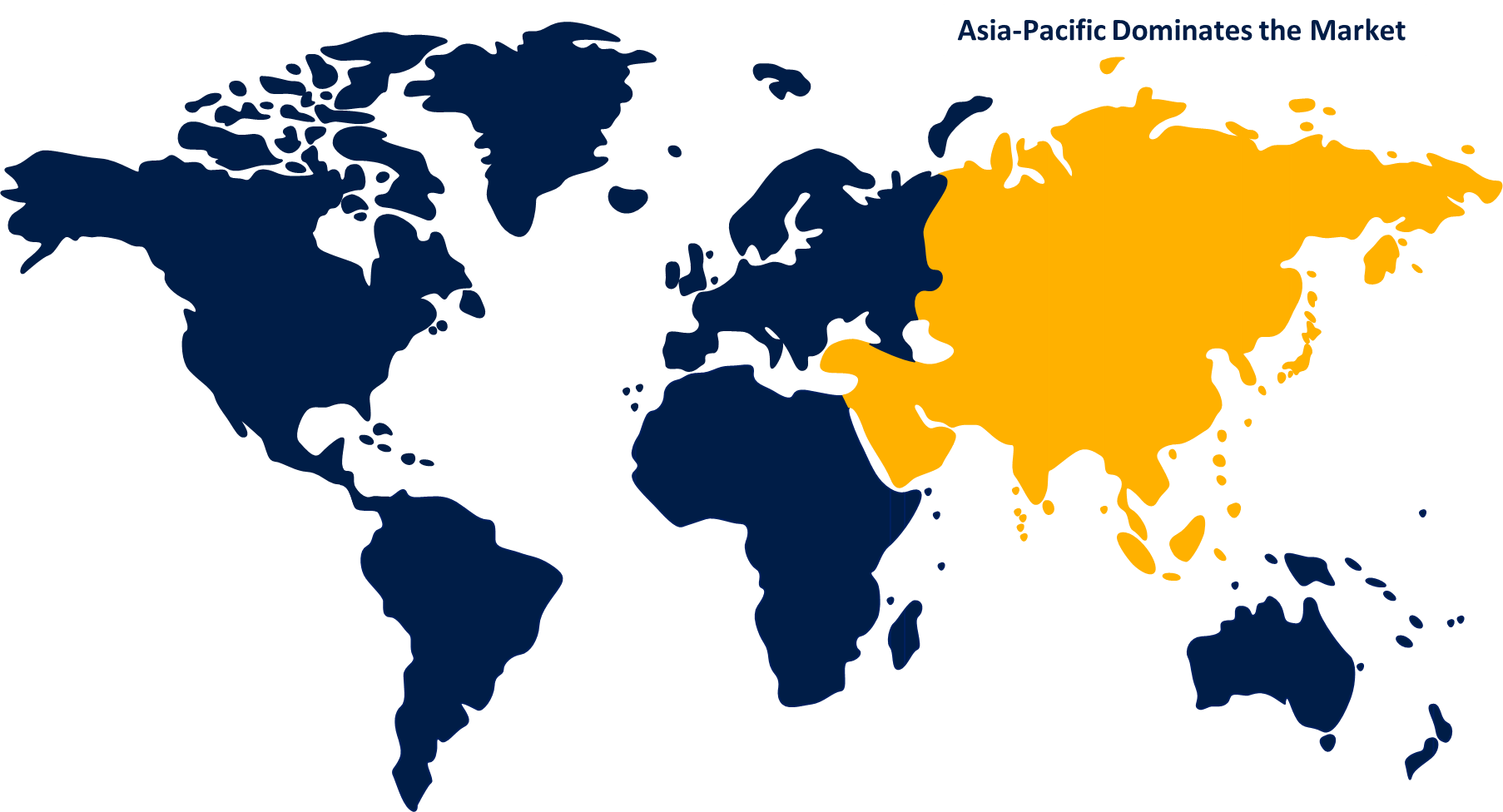
Asia-Pacific emerged as the largest market for the global atomic layer deposition market, with a market share of around 38.5% and 1.7 billion of the market revenue in 2021.
- In 2021, Asia- Pacific emerged as the largest market for the global atomic layer deposition market, with a market share of around 38.5% and 1.7 billion of the market revenue. Because the economies host a number of electronics industries. Additionally, it is anticipated that increased government expenditure on infrastructure development will have a positive effect on the market expansion in this region by luring leading electronics and automotive manufacturers to set manufacturing facilities in the area. The demand for deposition technologies has decreased as a result of the established electronics manufacturing bases in South Korea, China, and Taiwan. The expansion of this region has been supported by the proliferation of electronics product manufacturing, incredible modernization, expanding economies, and rising consumer electronics consumption.
- The North America market is expected to grow at the fastest CAGR between 2021 and 2030, the expanding number of solar energy projects and data centers constructed across the U.S. to meet the need for renewable and sustainable energy sources is fueling the development of Li-ion batteries and solar systems in the region.
Competitive Landscape
The report offers the appropriate analysis of the key organizations/companies involved within the global atomic layer deposition market along with a comparative evaluation primarily based on their product offering, business overviews, geographic presence, enterprise strategies, segment market share, and SWOT analysis. The report also provides an elaborative analysis focusing on the companies' current news and developments, including product development, innovations, joint ventures, partnerships, mergers & acquisitions, strategic alliances, and others. This allows for the evaluation of the overall competition within the market.
List of Key Market Players:
- Forge Nano Inc.
- Beneq Group
- Oxford Instruments plc
- The Kurt J. Lesker Company
- Pico sun Oy
- SENTECH Instruments GmbH
- Arradiance, LLC
- NCD Co. Ltd.
- Lam Research Corporation
- ASM International
- Applied Materials, Inc.
- Veeco Instruments Inc.
- CVD Equipment Corporation
Key Target Audience
- Market Players
- Investors
- End-users
- Government Authorities
- Consulting And Research Firm
- Venture capitalists
- Third-party knowledge providers
- Value-Added Resellers (VARs)
Some of the Key Developments:
- In July 2021, Picosun Group has partnered with Hermes-Epitek Corporation Ptv in order to broaden its network of international sales and service partners. One of the largest distributors of high-tech equipment in the world is Hermes-Epitek Corporation, with headquarters in Taiwan.
- In June 2021, The Kurt J. Lesker Company has created conformal atomic layer deposition (ALD) processes based on titanium (IV) oxide (TiO2) thin-film processes on Polymethyl Methacrylate (PMMA), exhibiting excellent surface and mechanical properties for potential engineering, medical, and biomedical applications.
- In March 2021, Canon and Tokyo Electron collaborate to join Japan's cutting-edge chipmaking initiative. Tokyo Electron, a Japanese supplier of chip manufacturing equipment, Canon, a company that creates semiconductor lithography equipment, and Screen Semiconductor Solutions, a company that produces wafer-coating and cleaning equipment, are all involved in the endeavor.
Market Segment
This study forecasts global, regional, and country revenue from 2019 to 2030. Spherical Insights has segmented the global atomic layer deposition market based on the below-mentioned segments:
Global Atomic Layer Deposition Market, By Product Type
- Metal ALD
- Aluminium Oxide ALD
- Catalytic ALD
- Plasma Enhanced ALD
- Others
Global Atomic Layer Deposition Market, By Application
- Electronics & Semiconductors
- Medical Equipment
- Research & Development Facilities
- Fuel Cells
- Solar Devices
- Magnetic Heads
- Sensors
- Barrier Layers
- Primer Layers
- Optical Devices
- Thermoelectric Materials
- Non—IC Application
- Others
Global Atomic Layer Deposition Market, Regional Analysis
- North America
- US
- Canada
- Mexico
- Europe
- Germany
- Uk
- France
- Italy
- Spain
- Russia
- Rest of Europe
- Asia Pacific
- China
- Japan
- India
- South Korea
- Australia
- Rest of Asia Pacific
- South America
- Brazil
- Argentina
- Rest of South America
- Middle East & Africa
- UAE
- Saudi Arabia
- Qatar
- South Africa
- Rest of Middle East & Africa
Frequently Asked Questions (FAQ)
-
What is the market size of the Atomic Layer Deposition market?As per Spherical Insights, the size of the Atomic Layer Deposition market was valued at USD 1.7 billion in 2022 to USD 4.90 billion by 2030.
-
What is the market growth rate of the Atomic Layer Deposition market?The Atomic Layer Deposition market is growing at a CAGR of 12.5% from 2022 to 2030.
-
Which country dominates the Atomic Layer Deposition market?Asia-Pacific emerged as the largest market for Atomic Layer Deposition.
-
Who are the key players in the Atomic Layer Deposition market?Key players in the Atomic Layer Deposition market are Forge Nano Inc., Beneq Group, Oxford Instruments plc, The Kurt J. Lesker Company, Pico sun Oy, SENTECH Instruments GmbH, Arradiance, LLC, NCD Co. Ltd., Lam Research Corporation, ASM International, Applied Materials, Inc., Veeco Instruments Inc., and CVD Equipment Corporation.
-
Which factor drives the growth of the Atomic Layer Deposition market?High demand for microelectronics will drive the market's growth over the forecast period.
Need help to buy this report?