Top 50 Companies in Plasma Enhanced Cvd Equipment (2025–2035): Competitive Analysis and Forecast
RELEASE DATE: Sep 2025 Author: Spherical InsightsRequest Free Sample Speak to Analyst
Description
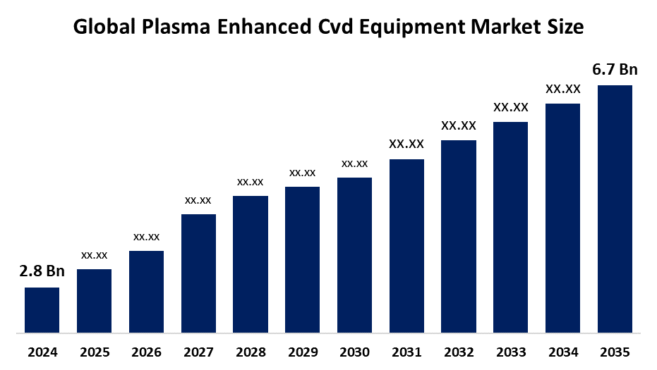
According to a research report published by Spherical Insights & Consulting, The Global Plasma Enhanced Cvd Equipment Market Size is projected to Grow from USD 2.8 Billion in 2024 to USD 6.7 Billion by 2035, at a CAGR of 8.25% during the forecast period 2025–2035. The market for plasma-enhanced CVD equipment is in greater demand because it enables high uniformity and high-quality thin-film deposition at lower temperatures, which is essential for solar cells, OLED displays, and advanced semiconductors. Because of its accuracy and adaptability, PECVD is a crucial facilitator of the growing demand from IoT, renewable energy, and display technologies.
Introduction
Plasma enhanced chemical vapor deposition (PECVD) is a type of deposition equipment that utilizes a plasma to enhance or activate the chemical reactions of gaseous precursors, thereby generating thin coatings on substrates. The market for plasma enhanced chemical vapor deposition systems is expanding quickly due to demand from Optoelectronics, solar energy, semiconductor manufacturing, and displays. The requirement for ultra-thin dielectric and passivation layers is increased by semiconductor chip scaling, i.e, sub 10 nm logic and memory, and PECVD's capacity to deposit high quality films at lower temperatures is essential for this. PECVD is used for passivation and anti-reflective coatings in solar modules, particularly high kinds like TOPCon and heterojunction. PECVD is also used by the display industry for barrier films and encapsulation. Despite the robust expansion, there are still obstacles to overcome, such as expensive capital expenditures, intricate process management, equipment upkeep, and a lack of skilled workers to operate these sophisticated machines.
Navigate Future Markets with Confidence: Insights from Spherical Insights LLP
The insights presented in this blog are derived from comprehensive market research conducted by Spherical Insights LLP, a trusted advisory partner to leading global enterprises. Backed by in-depth data analysis, expert forecasting, and industry-specific intelligence, our reports empower decision-makers to identify strategic growth opportunities in fast-evolving sectors. Clients seeking detailed market segmentation, competitive landscapes, regional outlooks, and future investment trends will find immense value in the full report. By leveraging our research, businesses can make informed decisions, gain a competitive edge, and stay ahead in the transition toward sustainable and profitable solutions.
Unlock exclusive market insights-Download the Brochure now and dive deeper into the future of the Plasma Enhanced Cvd Equipment Market.
Plasma Enhanced Cvd Equipment Market Size & Statistics
- The Market Size for Plasma Enhanced Cvd Equipment Was Estimated to be worth USD 2.8 Billion in 2024.
- The Market Size is Going to Expand at a CAGR of 8.25% between 2025 and 2035.
- The Global Plasma Enhanced Cvd Equipment Market Size is anticipated to reach USD 6.7 Billion by 2035.
- North America is expected to generate the highest demand during the forecast period in the Plasma Enhanced Cvd Equipment Market
- Asia Pacific is expected to grow the fastest during the forecast period in the Plasma Enhanced Cvd Equipment Market.
Regional growth and demand
Asia Pacific is expected to grow the fastest during the forecast period in the plasma enhanced CVD equipment market. The market for plasma enhanced CVD equipment is now growing in the Asia Pacific because of the region's supremacy in semiconductor manufacturing, especially in nations like South Korea, Taiwan, and China. Improved PECVD systems are required to produce next-generation microchips. Furthermore, the need for PECVD technology to improve solar cell efficiency is fueled by the quick growth of solar photovoltaic installations, particularly in China and India.
North America is expected to generate the highest demand during the forecast period in the plasma enhanced CVD equipment market. The plasma enhanced CVD equipment market with the quickest rate of growth throughout the study period is anticipated to be in North America, driven by a strong emphasis on innovation, sophisticated manufacturing capabilities, and the presence of top semiconductor, renewable energy, and automotive companies. With the help of federal programs encouraging the use of clean energy and domestic semiconductor manufacturing, the US, in particular, contributes significantly to the demand for PECVD systems. Research & development operations are also concentrated in North America, where a large number of academic institutions, research centers, and tech startups are propelling PEC innovation.
Top 10 trends in the Plasma Enhanced Cvd Equipment Market
- Surge in Semiconductor Demand
- Expansion in Advanced Packaging and Display Fabrication
- Integration of Artificial Intelligence and Automation
- Shift Towards Energy Efficient and Sustainable Practices
- Advancements in Thin Film Solar Cell Production
- Regional Market Dynamics
- Technological Innovations in PECVD Systems
- Development of Multi Chamber Systems
- Regulatory and Trade Influences
- Emergence of Hybrid CVD Systems
1. Surge in Semiconductor Demand
The market for plasma enhanced chemical vapor deposition equipment is being greatly impacted by the increase in demand for semiconductors. Technological developments like artificial intelligence, 5G, and the Internet of Things are driving this growing demand since they call for more sophisticated semiconductor devices. Because PECVD systems make it possible to deposit thin films that are necessary for integrated circuits, they are fundamental to the manufacturing of these devices. As a result, in order to satisfy the rising demand for high-performance chips, semiconductor firms are spending money on sophisticated PECVD equipment. As the need for increasingly complex semiconductor devices rises, this tendency is anticipated to continue.
2. Expansion in Advanced Packaging and Display Fabrication
Equipment for plasma enhanced chemical vapor deposition is in high demand due to the growth of sophisticated packaging and display production. PECVD systems play a key role in advanced packaging by depositing low stress dielectric films, like silicon oxide and silicon nitride, which are necessary for fan out wafer level packaging and through-silicon via isolation. By combining several chips into a single package, these procedures improve performance while decreasing size. PECVD is used for thin film encapsulation in display production, especially for OLED and microLED technologies. It creates oxygen and moisture barrier layers that shield the organic materials from deterioration, increasing the displays' longevity and dependability.
3. Integration of Artificial Intelligence and Automation
The production of semiconductors is being revolutionized by the incorporation of automation and artificial intelligence into plasma enhanced chemical vapor deposition systems. By evaluating vast datasets to maximize deposition quality, AI systems increase process control, resulting in better film uniformity and less material waste. Automation reduces waste and downtime by facilitating real-time monitoring and diagnostics, which enables prompt responses to process irregularities. Furthermore, sophisticated robotic systems with vision assisted technology guarantee accurate wafer handling, making up for thermal shrinkage and manufacturing tolerances. This greatly increases productivity and dependability when working with delicate substrates. Together, these developments improve PECVD techniques scalability, accuracy, and efficiency while satisfying the expanding needs of contemporary semiconductor applications.
4. Shift Towards Energy Efficient and Sustainable Practices
The production of semiconductors is changing as a result of the move to sustainable and energy-efficient methods in plasma enhanced chemical vapor deposition. PECVD systems are notoriously energy-intensiveve they can consume as much as 60% of the electricity used in a semiconductor fab. Manufacturers are responding to this by implementing cutting-edge technologies like pulsed plasma operation, which can lower energy requirements by as much as 30%. In order to lessen the impact on the environment and increase the efficiency of deposition, the switch to sustainable gases like hydrogen and nitrogen is also being investigated. To reduce waste and water consumption, closed loop water recycling technologies are also being used. These programs push the semiconductor industry toward more environmentally friendly production methods by being in line with international sustainability objectives and regulatory demands.
5. Advancements in Thin Film Solar Cell Production
The efficiency and adaptability of photovoltaic technologies are being greatly increased by developments in the manufacturing of thin film solar cells. High quality amorphous silicon and silicon nitride films may be deposited due to plasma enhanced chemical vapor deposition, which is essential to this advancement. By acting as passivation layers, these films enhance device performance by lowering surface recombination. Cutting edge methods like peel-and-stick and roll to roll manufacturing are making it easier to combine thin film solar cells onto flexible substrates, expanding their use in fields like portable electronics and building integrated photovoltaics. Energy yield is also being increased by 20–30% due to the development of bifacial modules, which gather sunlight from both sides. All of these developments are driving thin-film solar cells closer to greater efficiency and wider use in the renewable energy industry.
Empower your strategic planning:
Stay informed with the latest industry insights and market trends to identify new opportunities and drive growth in the plasma enhanced CVD equipment market. To explore more in-depth trends, insights, and forecasts, please refer to our detailed report.
Top 25 Companies Leading the Plasma Enhanced Cvd Equipment Market
- Applied Materials
- ASM International
- Lam Research
- Tokyo Electron Limited (TEL)
- Kokusai Electric
- Wonik IPS
- Meyer Burger
- Centrotherm
- Tempress
- Plasma Therm
- C New Energy Technology
- Jusung Engineering
- KLA Tencor (Orbotech)
- ULVAC, Inc.
- Beijing NAURA
- Shenyang Piotech
- Oxford Instruments
- SAMCO
- CVD Equipment Corporation
- Trion Technology
- SENTECH Instruments
- NANO MASTER
- AIXTRON SE
- Plasma Etch, Inc.
- Nordson Corporation
- Others
1. Applied Materials
Headquarters: Santa Clara, California
Applied Materials is a world leader in materials engineering solutions, with its headquarters located in Santa Clara, California. The company uses its technological superiority to increase productivity and sustainability by offering manufacturing equipment, services, and software to semiconductor and display manufacturers. With a substantial presence in India, including Bengaluru, Chennai, Mumbai, Coimbatore, and Pune, Applied Materials is a global business. The organization contributes to the expanding technology sector in India by concentrating on business intelligence, data management, and analytics. In keeping with India's strategic goal of becoming a major player in the global semiconductor supply chain, Applied Materials is aggressively looking into partnerships with businesses engaged in semiconductor projects in that country.
2. ASM International
Headquarters: Almere, Netherlands
The headquarters of the Dutch multinational company ASM International N.V. are located in Almere, Netherlands. With an emphasis on deposition techniques like atomic layer deposition, chemical vapor deposition, and epitaxy, the company specializes in creating and producing equipment for semiconductor production. Advanced semiconductor devices utilized in consumer electronics, automotive systems, and artificial intelligence are all made possible due in large part to ASM's technology. ASM is a multinational corporation that runs research and development facilities in places including Helsinki, Leuven, Phoenix, Tama, and Dongtan. The business supports its vast range of global clients with production sites in South Korea and Singapore. Because of its dedication to quality and innovation, ASM has established itself as a major force in the semiconductor equipment sector.
3. Lam Research
Headquarters: Fremont, California
Lam Research Corporation is an American company that supplies the semiconductor industry with wafer-fabrication equipment and associated services. Front end wafer processing, which includes the processes that produce the active parts of semiconductor devices, i.e., transistors, capacitors, and their wiring, i.e, interconnects, is the main application for its products. Additionally, the business manufactures equipment for the back-end wafer level packaging sector as well as associated manufacturing areas like microelectromechanical systems.
4. Tokyo Electron Limited (TEL)
Headquarters: Tokyo, Japan
The headquarters of Tokyo Electron Limited, a well-known producer of semiconductor equipment in Japan, are located in Minato ku's Akasaka Biz Tower. The business focuses on creating, producing, and marketing equipment for the production of semiconductors, such as etching, cleaning, and deposition systems. With 26 businesses spread over 18 nations and regions, TEL runs a global network that includes 95 locations. To assist semiconductor projects, TEL is growing its footprint in India by opening new offices in Dholera, Gujarat, and Assam. TEL is also establishing a new development center in Bengaluru to enhance India's position in the world supply chain for semiconductors.
5. Kokusai Electric
Headquarters: Tokyo, Japan
The headquarters of the Japanese semiconductor equipment manufacturer Kokusai Electric Corporation are located in Chiyoda, Tokyo. The business focuses on creating and manufacturing tools for processing semiconductor wafers, such as etching and deposition systems. Kokusai Electric has a number of technology and production facilities in Japan, including the Tonami Production Center and the Toyama Technology & Manufacturing Center. Through Kokusai Electric Korea Co., Ltd., the firm also has a substantial presence in South Korea, with facilities located in Pyeongtaek, Dongtan, Godeok, Icheon, and Cheongju. These sites help Kokusai Electric's worldwide operations and further its position in the semiconductor sector.
Are you ready to discover more about the plasma enhanced CVD equipment market?
The report provides an in-depth analysis of the leading companies operating in the global plasma enhanced CVD equipment market. It includes a comparative assessment based on their product portfolios, business overviews, geographical footprint, strategic initiatives, market segment share, and SWOT analysis. Each company is profiled using a standardized format that includes:
Company Profiles
- Applied Materials
- Business Overview
- Company Snapshot
- Products Overview
- Company Market Share Analysis
- Company Coverage Portfolio
- Financial Analysis
- Recent Developments
- Merger and Acquisitions
- SWOT Analysis
- ASM International
- LAM RESEARCH
- Tokyo Electron Limited (TEL)
- Kokusai Electric
- JDA Software
- Epicor Software Corporation
- TECSYS
- Made4net
- Others
Conclusion
The Plasma Enhanced CVD Equipment Market Size is accelerating due to the advancements in the semiconductor industry, specifically the need for high performance, compact devices. The need for PECVD in the manufacturing of thin-film solar cells is also being increased by the growing emphasis on renewable energy sources, particularly solar energy. The market is growing as a result of new wear-resistant coating applications in sectors including aerospace and automotive. PECVD is a key component of improved semiconductor materials, which are becoming more and more necessary as smart technologies and Internet of Things devices proliferate. PECVD technology advancements, such as eco-friendly materials and more effective procedures, are opening up new business prospects.
About the Spherical Insights & Consulting
Spherical Insights & Consulting is a market research and consulting firm which provides actionable market research study, quantitative forecasting and trends analysis provides forward-looking insight especially designed for decision makers and aids ROI.
Which is catering to different industry such as financial sectors, industrial sectors, government organizations, universities, non-profits and corporations. The company's mission is to work with businesses to achieve business objectives and maintain strategic improvements.
CONTACT US:
For More Information on Your Target Market, Please Contact Us Below:
Phone: +1 303 800 4326 (the U.S.)
Phone: +91 90289 24100 (APAC)
Email: inquiry@sphericalinsights.com, sales@sphericalinsights.com
Contact Us: https://www.sphericalinsights.com/contact-us
Need help to buy this report?