World’s Top 20 Industries in Laser Mass Transfer Equipment Market 2025 Watchlist: Statistical Report (2024–2035)
RELEASE DATE: Sep 2025 Author: Spherical InsightsRequest Free Sample Speak to Analyst
Description
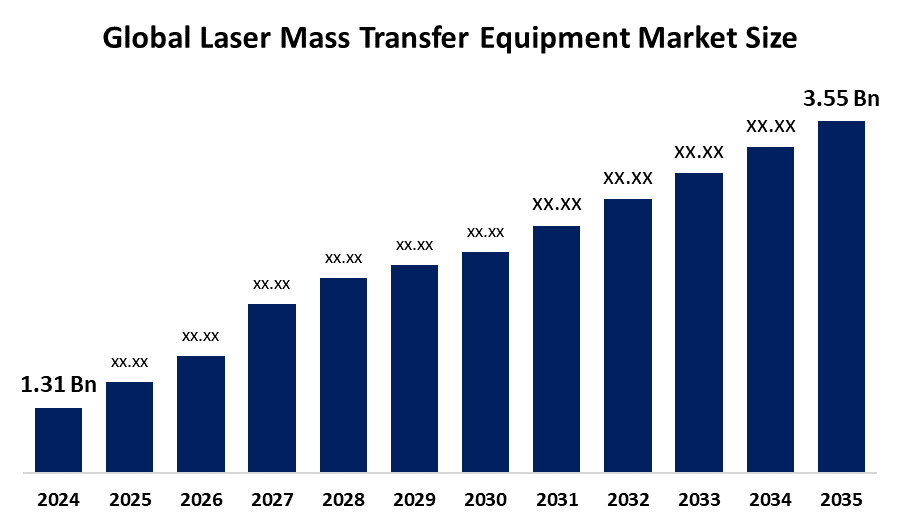
According to a research report published by Spherical Insights & Consulting, The Global Laser Mass Transfer Equipment Market Size is projected To Grow from USD 1.31 Billion in 2024 to USD 3.55 Billion by 2035, at a CAGR of 9.49% during the forecast period 2025–2035. This strong growth results from rising demand in multiple high-tech manufacturing sectors, such as semiconductor, display, and photovoltaic manufacturing, fueled by continuous trends of miniaturisation and elevated precision needs in production processes.
Introduction
The Worldwide Laser Mass Transfer Equipment Market Size refers to the area of precision manufacturing technology that specialises in devices employing sophisticated laser systems to move materials, like semiconductor dies, micro-LEDs, or functional coatings, from a source substrate to a target substrate with exceptional accuracy and efficiency. This technology is crucial in semiconductor packaging, electronics assembly, advanced display production (such as micro-LED and OLED), biomedical devices, and additive manufacturing. Laser mass transfer systems utilise different laser types (such as pulsed, continuous-wave, and ultrafast) along with precise motion control to attain sub-micron placement precision, increased throughput, and minimised material waste. Essential features comprise swift material layering, adaptable patterns, and suitability for small and fragile elements. The market is swiftly growing due to developments in semiconductor packaging (including 3D stacking and System-in-Package), high-performance computing, and smaller electronics that increase the need for enhanced precision.
Navigate Future Markets with Confidence: Insights from Spherical Insights LLP
The insights presented in this blog are derived from comprehensive market research conducted by Spherical Insights LLP, a trusted advisory partner to leading global enterprises. Backed by in-depth data analysis, expert forecasting, and industry-specific intelligence, our reports empower decision-makers to identify strategic growth opportunities in fast-evolving sectors. Clients seeking detailed market segmentation, competitive landscapes, regional outlooks, and future investment trends will find immense value in the full report. By leveraging our research, businesses can make informed decisions, gain a competitive edge, and stay ahead in the transition toward sustainable and profitable solutions.
Unlock exclusive market insights - Download the Brochure now and dive deeper into the future of the Laser Mass Transfer Equipment Market.
Laser Mass Transfer Equipment Market Size & Statistics
- The Market Size for Laser Mass Transfer Equipment Was Estimated to be worth USD 1.31 Billion in 2024.
- The Market Size is Going to Expand at a CAGR of 9.49% between 2025 and 2035.
- The Global Laser Mass Transfer Equipment Market Size is anticipated to reach USD 3.55 Billion by 2035.
- Asia Pacific is estimated to generate the highest demand during the forecast period in The Laser Mass Transfer Equipment Market.
- Europe is anticipated to grow the fastest over the forecast period in The Laser Mass Transfer Equipment Market.
Regional growth and demand
Europe is projected to grow at the fastest CAGR during the forecast period in the laser mass transfer equipment market. Europe is fueled by the region's emphasis on cutting-edge manufacturing and technological progress. Further, Germany, France, and the United Kingdom play vital roles in market expansion, boasting strong sectors in automotive, aerospace, and electronics. The region's significant focus on renewable energy and sustainability is also increasing the need for precision manufacturing solutions in the creation of photovoltaic components.
Asia Pacific is anticipated to grow at the highest rate during the forecast period in the laser mass transfer equipment market. The laser mass transfer equipment market is fueled by significant electronics and semiconductor manufacturing centres in nations like China, Japan, South Korea, and others. Further, the robust industrial foundation of the region, along with substantial investments in advanced manufacturing infrastructure, is propelling the uptake of laser mass transfer technologies. Moreover, beneficial government policies and incentives for the electronics and semiconductor sectors are further enhancing market growth in the Asia Pacific region.
Top 10 trends in the Laser Mass Transfer Equipment Market
- High-Speed and High Throughput Solutions
- The Move to Higher Precision and Tighter Tolerances
- Integrated and Automated Systems
- Specialisation for Different Applications
- Advanced Laser Technologies
- Focus on Defect Management and Yield Improvement
- Hybrid Transfer Technologies
- Development of Sustainable Manufacturing Processes
- Increased Investment in R&D and Strategic Partnerships
- The Rise of Transfer-Free or All-in-One Solutions
1. Integrated and Automated Systems
To cut expenses and enhance output, producers are shifting from independent machinery. The movement is towards completely automated, cohesive systems capable of executing several process stages within one device. This encompasses not only the mass transfer itself but also pre-transfer checks, post-transfer checks, and repair functions, all integrated into a single cohesive platform.
2. Specialisation for Different Applications
The market is divided according to the application. The technology for large-format displays (such as TVs and digital signage) demands distinct specifications for speed and throughput compared to the technology for high pixel density microdisplays (like those found in AR/VR headsets). This is resulting in the creation of tailored tools designed for particular applications.
3. Advanced Laser Technologies
Advancements in laser technology represent a significant trend. Producers are investigating various laser types, such as femtosecond and picosecond lasers, to enhance the accuracy of the transfer procedure. These sophisticated lasers can deliver cleaner cuts and minimise the thermal effect on the small LED chips, which is essential for preserving their performance and yield.
4. Hybrid Transfer Technologies
Although laser-based transfer remains a prominent technique, the market is simultaneously investigating and incorporating hybrid solutions. This encompasses systems that merge laser-induced transfer with additional techniques, like electrostatic or fluidic assembly. These combined methods aim to utilise the strengths of each technology to address particular obstacles and attain greater outputs.
5. Increased Investment in R&D and Strategic Partnerships
The Micro LED sector is still emerging, featuring intense competition and significant R&D funding. Key companies in the semiconductor and display equipment sectors are either creating their own exclusive technologies or establishing strategic alliances to speed up the market introduction of their offerings. This is resulting in swift technological progress and a vibrant, competitive environment.
Empower your strategic planning:
Stay informed with the latest industry insights and market trends to identify new opportunities and drive growth in the laser mass transfer equipment market. To explore more in-depth trends, insights, and forecasts, please refer to our detailed report.
Top 20 Companies Leading the Laser Mass Transfer Equipment Market
- Applied Materials Inc.
- ASML Holding N.V.
- Lam Research Corporation
- KLA Corporation
- Tokyo Electron Limited
- Hitachi High-Technologies Corporation
- SCREEN Holdings Co., Ltd.
- Nikon Corporation
- Canon Inc.
- Advantest Corporation
- Onto Innovation Inc.
- Veeco Instruments Inc.
- Rudolph Technologies, Inc.
- ASM International N.V.
- Kulicke & Soffa Industries, Inc.
- Plasma-Therm LLC
- EV Group (EVG)
- SUSS MicroTec SE
- Ultratech, Inc.
- MKS Instruments, Inc.
1. Applied Materials Inc.
Headquarters: Santa Clara, California, USA
Applied Materials, Inc. is a prominent American multinational company offering manufacturing tools, services, and software for the semiconductor, flat panel display, solar photovoltaic, and related sectors. Being among the biggest suppliers of semiconductor fabrication equipment globally, the company's business model relies on its profound knowledge in materials engineering, which encompasses the deposition, shaping, and removal of materials at the atomic scale. Applied Materials plays a crucial role in advanced technologies, demonstrating a robust dedication to R&D and offering a varied product lineup that assists its clients in developing the next wave of electronic devices. The organisation consists of three reportable divisions: Silicon Systems Group, Applied Global Services, and Display and Related Markets. The Display sector is especially significant to the laser mass transfer equipment market.
2. ASML Holding N.V.
Headquarters: Veldhoven, Netherlands
ASML Holding N.V. is a Netherlands-based global company and the top provider of photolithography systems for the semiconductor sector. Its business model focuses on delivering sophisticated and advanced machinery that is crucial for the manufacturing of integrated circuits (chips). ASML possesses a near-monopoly in the sector for extreme ultraviolet (EUV) lithography equipment, essential for producing the most advanced and tiniest chips utilised in contemporary electronics. ASML's primary business revolves around three key product categories: EUV lithography systems, deep ultraviolet (DUV) lithography systems, and a range of metrology, inspection, and software solutions that enhance lithography.
3. Lam Research Corporation
Headquarters: Fremont, California, USA
Lam Research Corporation is an American multinational company and a top global provider of wafer fabrication equipment and services for the semiconductor sector. The company's business approach focuses on supplying specialised equipment for several critical phases of chip manufacturing, such as thin film deposition, plasma etching, photoresist removal, and wafer cleaning. Lam's value proposition lies in its capacity to provide exceptional process performance and control at the atomic level, crucial for producing the intricate, 3D architectures of contemporary memory and logic chips. The products of the company are utilised in front-end wafer processing (producing the active parts) as well as back-end wafer-level packaging (linking the parts). Lam is an essential facilitator of the technologies that drive contemporary electronics, including mobile phones and artificial intelligence (AI) systems.
4. KLA Corporation
Headquarters: California, USA
KLA Corporation is a U.S.-based multinational company and a prominent global provider of process control and yield management systems for the semiconductor, flat panel display, and various nanoelectronics sectors. The business model of the company focuses on offering sophisticated inspection, metrology, and data analytics tools that assist manufacturers in detecting and rectifying defects, measuring vital parameters, and enhancing overall production yield. KLA's value proposition lies in its capacity to offer a complete array of solutions that are critical for the large-scale manufacturing of intricate electronic devices. Its systems are applied at each phase of the manufacturing process, from research and development to the packaging of the final product.
5. Tokyo Electron Limited
Headquarters: Akasaka Biz Tower, Tokyo, Japan
Tokyo Electron Limited (TEL) is a Japanese global corporation and a leader in producing equipment for semiconductor and flat panel display (FPD) manufacturing. The business model of the company focuses on offering a diverse assortment of specialised and innovative tools crucial for the production of integrated circuits, FPDs, and solar cells. TEL is recognised for its significant market presence in various critical process stages, such as coater/developers, plasma etching systems, and thermal processing systems. The value proposition of the company is rooted in its significant R&D efforts, worldwide presence, and capacity to offer complete, integrated solutions for its clients. For example, a key segment of TEL's operations centres on advanced packaging and 3D integration technologies, including wafer bonding and debonding systems (e.g., its Synapse series).
Are you ready to discover more about the laser mass transfer equipment market?
The report provides an in-depth analysis of the leading companies operating in the global laser mass transfer equipment market. It includes a comparative assessment based on their product portfolios, business overviews, geographical footprint, strategic initiatives, market segment share, and SWOT analysis. Each company is profiled using a standardized format that includes:
Company Profiles
- Applied Materials Inc.
- Business Overview
- Company Snapshot
- Products Overview
- Company Market Share Analysis
- Company Coverage Portfolio
- Financial Analysis
- Recent Developments
- Merger and Acquisitions
- SWOT Analysis
- ASML Holding N.V.
- Lam Research Corporation
- KLA Corporation
- Tokyo Electron Limited
- Hitachi High-Technologies Corporation
- SCREEN Holdings Co., Ltd.
- Nikon Corporation
- Canon Inc.
- Advantest Corporation
- Onto Innovation Inc.
- Veeco Instruments Inc.
- Rudolph Technologies, Inc.
- ASM International N.V.
- Kulicke & Soffa Industries, Inc.
- Plasma-Therm LLC
- EV Group (EVG)
- SUSS MicroTec SE
- Ultratech, Inc.
- MKS Instruments, Inc.
- Others
Conclusion
The Global Laser Mass Transfer Equipment Market Size is anticipated to expand notably from USD 1.31 billion in 2024 to USD 3.55 billion by 2035, reflecting a CAGR of 9.49%. The rising demand for high-precision manufacturing technologies in semiconductor packaging, advanced display production (such as micro-LED, OLED), photovoltaic manufacturing, and biomedical devices primarily drives this growth. The market gains advantages from trends including miniaturisation, Industry 4.0 automation, and sophisticated laser technologies such as femtosecond and picosecond lasers, which allow for increased precision and efficiency. Asia Pacific is projected to create the largest demand because of major electronics and semiconductor production centres in China, Japan, and South Korea, bolstered by government support. Europe is expected to expand at the quickest pace, driven by a focus on advanced manufacturing in nations like Germany, France, and the UK, as well as an emphasis on renewable energy innovations.
About the Spherical Insights & Consulting
Spherical Insights & Consulting is a market research and consulting firm which provides actionable market research study, quantitative forecasting and trends analysis provides forward-looking insight especially designed for decision makers and aids ROI.
Which is catering to different industry such as financial sectors, industrial sectors, government organizations, universities, non-profits and corporations. The company's mission is to work with businesses to achieve business objectives and maintain strategic improvements.
CONTACT US:
For More Information on Your Target Market, Please Contact Us Below:
Phone: +1 303 800 4326 (the U.S.)
Phone: +91 90289 24100 (APAC)
Email: inquiry@sphericalinsights.com, sales@sphericalinsights.com
Contact Us: https://www.sphericalinsights.com/contact-us
Need help to buy this report?