Top 20 Companies in Semiconductor and IC Packaging Materials Market Worldwide 2025: Statistical View by Spherical Insights and Consulting
RELEASE DATE: Sep 2025 Author: Spherical InsightsRequest Free Sample Speak to Analyst
Description
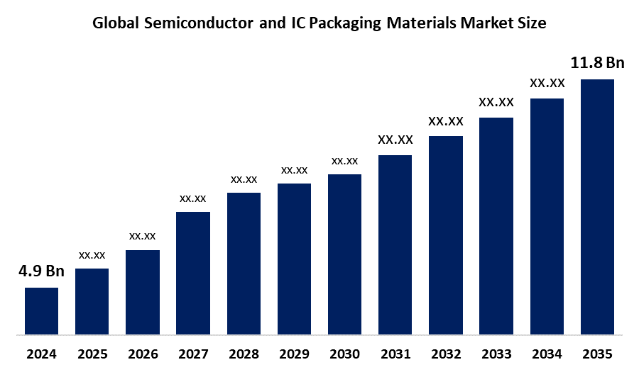
According to a research report published by Spherical Insights & Consulting, The Global Semiconductor and IC Packaging Materials Market Size is projected To Grow from USD 4.9 Billion in 2024 to USD 11.8 Billion by 2035, at a CAGR of 8.32% during the forecast period 2025–2035. The development of the semiconductor and IC packaging materials market is being driven by increasing demand for miniaturized electronics, 5G deployment, AI adoption, electric vehicles, and robust government encouragement of domestic chip manufacturing.
Introduction
The Semiconductor And IC Packaging Materials Market Size refers to the sector focused on materials used to cover and protect integrated circuits (ICs), facilitate electrical contact, control thermal properties, and provide structural support. These products include lead frames, substrates, wire bonds, encapsulants, and die attach compounds. They are mainly used in consumer electronics, industrial, automotive, and communications devices. Market expansion is driven by the high growth rate of the electronics sector, the implementation of 5G, AI, IoT, and electric vehicles, all of which necessitate miniaturized and complex semiconductor devices. One of the key strengths in the industry is its constant innovation and adoption of effective packaging solutions, such as 3D ICs and system in package (SiP) technologies. Opportunities are expanding as the uptake of smart devices and automation increases, particularly in emerging markets. Governments worldwide are financing semiconductor manufacturing and implementing policy measures to reduce dependence on foreign supply chains, as seen in the American case. CHIPS Act and similar programs in the EU, China, and India. Programs will be anticipated to support domestic manufacturing and drive further market growth.
Navigate Future Markets with Confidence: Insights from Spherical Insights LLP
The insights presented in this blog are derived from comprehensive market research conducted by Spherical Insights LLP, a trusted advisory partner to leading global enterprises. Backed by in-depth data analysis, expert forecasting, and industry-specific intelligence, our reports empower decision-makers to identify strategic growth opportunities in fast-evolving sectors. Clients seeking detailed market segmentation, competitive landscapes, regional outlooks, and future investment trends will find immense value in the full report. By leveraging our research, businesses can make informed decisions, gain a competitive edge, and stay ahead in the transition toward sustainable and profitable solutions.
Unlock exclusive market insights - Download the Brochure now and dive deeper into the future of the Semiconductor and IC Packaging Materials Market.
Semiconductor and IC Packaging Materials Market Size & Statistics
- The Market Size for Semiconductor and IC Packaging Materials Was Estimated to be worth USD 4.9 Billion in 2024.
- The Market Size is Going to Expand at a CAGR of 8.32% between 2025 and 2035.
- The Global Semiconductor and IC Packaging Materials Market Size is anticipated to reach USD 11.8 Billion by 2035.
- Asia Pacific is expected to generate the largest demand during the forecast period in the Semiconductor and IC Packaging Materials Market
- North America is expected to grow the fastest during the forecast period in the Semiconductor and IC Packaging Materials Market.
Regional growth and demand
North America is expected to grow the fastest during the forecast period in the semiconductor and IC packaging materials market. North America is the most rapidly growing region in the semiconductor and IC packaging materials market, owing to improved government support through the CHIPS Act, growing local semiconductor manufacturing investments, technological developments in packaging, and moving away from dependency on Asia through reshoring production capacity.
Asia Pacific is expected to generate the largest demand during the forecast period in the semiconductor and IC packaging materials market. Asia Pacific is the dominating market for semiconductor and IC packaging materials due to its leading semiconductor production ecosystem with powerful players in Taiwan, China, South Korea, and Japan. It benefits low-cost manufacturing, a robust supply chain infrastructure, high demand for consumer electronics, and ongoing investments from the government to drive industry expansion and technology advancements.
Top 10 trends in the Semiconductor and IC Packaging Materials Market
- Miniaturization and advanced packaging
- Rise of heterogeneous integration
- Thermal management innovations
- Shift towards eco-friendly materials
- AI and 5G driving material demand
- Advancements in substrate materials
- Government initiatives and domestic manufacturing
- Investment in advanced packaging equipment
- Focus on reliability and quality control
- Global supply chain diversification
1. Miniaturization and advanced packaging
Miniaturization generates demand for sophisticated IC packaging materials, which enable denser, faster, and more powerful chips by combining multiple functions and dissipating heat in compact packages. Sophisticated packaging materials must provide high electrical performance, thermal dissipation, and reliability to address these multifunctional, confined applications across various sectors.
2. Rise of heterogeneous integration
Heterogeneous integration integrates various disparate chip building blocks into a single next-generation package, thereby breaking the constraints of monolithic design. This trend creates opportunities for the demand for new semiconductor packaging materials and methods, such as chiplets and 3D stacking, to deliver improved performance, reduced form factors, and lower costs across applications ranging from AI to mobile.
3. Thermal management innovations
Innovations address the co-design of package and device, as well as next-generation packaging techniques such as 3D and 2.5D integration, to enhance heat dissipation. This is paramount in sustaining performance and reliability through heat control, which becomes essential as devices grow more complex and denser, particularly with wide bandgap (WBG) devices
4. Shift towards eco-friendly materials
The trend towards green materials in semiconductor and IC packaging includes embracing lead-free solders, halogen-free laminates, and bio-based polymers, thereby decreasing the environmental footprint while complying with regulatory requirements. This movement is conducive to sustainable manufacturing and aligns with the growing consumer demand for greener products.
5. AI and 5G driving material demand
5G and AI create demand for next-generation materials such as silicon carbide and gallium nitride, necessitating innovative, high-density packaging of miniaturized, effective chips utilized in 5G equipment and consumer devices. This growing trend increases materials such as thermal interface materials, encapsulants, and organic substrates, calling for smaller, more efficient packages to address the needs of developing technologies.
Empower your strategic planning:
Stay informed with the latest industry insights and market trends to identify new opportunities and drive growth in the semiconductor and IC packaging materials market. To explore more in-depth trends, insights, and forecasts, please refer to our detailed report.
Top 12 Companies Leading the Semiconductor and IC Packaging Materials Market
- DuPont
- BASF SE
- Henkel AG & Co. KGaA
- Hitachi Chemical
- Kyocera Corporation
- LG Chem
- Sumitomo Chemical
- Texas Instruments
- Samsung Electronics
- Tanaka Holdings
- Intel Corporation
- Toray Industries Corporation
1. DuPont
Headquarters: Wilmington, Delaware, USA
DuPont is a global leader in advanced materials and specialty chemicals. In the semiconductor and IC packaging materials market, DuPont plays a critical role by supplying a wide range of effective materials used in advanced packaging processes. These include dielectric materials, photoresists, thermal interface materials, adhesives, and encapsulants that support chip scaling, miniaturization, and acute performance. The company is also a key innovator in efficient materials for 5G, compact interconnects, and green formulations, aligning with sustainability and next-generation semiconductor technologies.
2. BASF SE
Headquarters: Ludwigshafen, Germany
BASF SE is one of the world’s leading chemical companies, actively contributing to the semiconductor and IC packaging materials market. BASF provides a broad portfolio of advanced materials, including photoresists, dielectrics, cleaning agents, encapsulants, and dopants, which are essential for precision and reliability in semiconductor packaging. The company focuses on developing refined materials that support miniaturization, thermal stability, and high-frequency performance. BASF is also investing in sustainable and bio-based solutions, aligning its innovations with global environmental and regulatory standards.
3. Henkel AG & Co. KGaA
Headquarters: Dusseldorf, Germany
Henkel AG & Co. KGaA is a global leader in adhesives, sealants, and functional coatings, with a strong presence in the semiconductor and IC packaging materials market. Henkel specializes in die attach adhesives, underfills, encapsulants, thermal interface materials, and solder pastes, all critical for device protection, thermal management, and reliability. The company is known for its focus on innovative, effective, and sustainable materials, supporting advanced packaging technologies such as radiative, SiP, and 3D integration in mobile, automotive, and industrial electronics.
4. Hitachi Chemical
Headquarters: Tokyo, Japan
Hitachi Chemical Co., Ltd. plays a significant role in the semiconductor and IC packaging materials market. The company provides a wide range of advanced materials, including die attach films, encapsulants, underfills, and photosensitive resins used in compact and robust packaging. Known for its innovation in organic and insulating materials, Hitachi Chemical supports advanced packaging methods such as radiative, flip chip, and wafer-level packaging, catering to mobile, automotive, and effective computing markets.
5. Kyocera Corporation
Headquarters: Kyoto, Japan
Kyocera Corporation is a key player in the semiconductor and IC packaging materials market, offering a diverse range of advanced materials and components. The company specializes in ceramic and organic package substrates, bonding materials, encapsulants, and thermal interface solutions. Kyocera supports various packaging technologies such as system in package (SiP) and flip chip packaging, serving sectors such as consumer electronics, automotive, and telecommunications. Its materials ensure high reliability, miniaturization, and superior thermal and electrical performance.
Are you ready to discover more about the semiconductor and IC packaging materials market?
The report provides an in-depth analysis of the leading companies operating in the global semiconductor and IC packaging materials market. It includes a comparative assessment based on their product portfolios, business overviews, geographical footprint, strategic initiatives, market segment share, and SWOT analysis. Each company is profiled using a standardized format that includes:
Company Profiles
- DuPont
- Business Overview
- Company Snapshot
- Products Overview
- Company Market Share Analysis
- Company Coverage Portfolio
- Financial Analysis
- Recent Developments
- Merger and Acquisitions
- SWOT Analysis
- BASF SE
- Henkel AG & Co. KGaA
- Hitachi Chemical
- Kyocera Corporation
- LG Chem
- Sumitomo Chemical
- Texas Instruments
- Samsung Electronics
- Others.
Conclusion
The IC and Semiconductor Packaging Materials Market Size involves materials such as lead frames, substrates, wire bonds, encapsulants, and die attach compounds that are utilized to protect and interconnect integrated circuits. The market is boosted by innovations in miniaturization, 3D ICs, and SiP technologies with the growth of 5G, AI, IoT, and EVs. The primary trends are green materials, thermal management, and heterogeneous integration. Market leaders such as DuPont, BASF, Henkel, Hitachi Chemical, and Kyocera provide innovative, green materials enabling effective and miniature semiconductor devices.
About the Spherical Insights & Consulting
Spherical Insights & Consulting is a market research and consulting firm which provides actionable market research study, quantitative forecasting and trends analysis provides forward-looking insight especially designed for decision makers and aids ROI.
Which is catering to different industry such as financial sectors, industrial sectors, government organizations, universities, non-profits and corporations. The company's mission is to work with businesses to achieve business objectives and maintain strategic improvements.
CONTACT US:
For More Information on Your Target Market, Please Contact Us Below:
Phone: +1 303 800 4326 (the U.S.)
Phone: +91 90289 24100 (APAC)
Email: inquiry@sphericalinsights.com, sales@sphericalinsights.com
Contact Us: https://www.sphericalinsights.com/contact-us
Need help to buy this report?